
Quantum Material


NewsFlash
September 12, 2024
Industry Pioneers
Editor's Picks
-

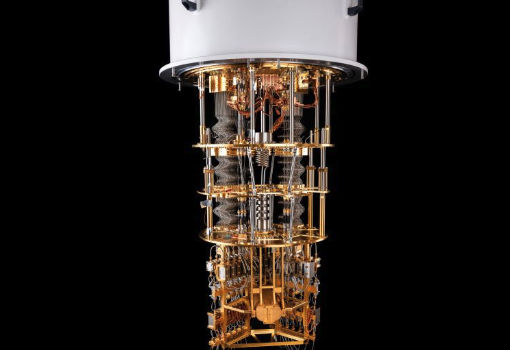
Qolab Announces $54.2 Million Series B Financing and Commitments Led by UC Investments
-

UOB and Singapore’s Centre for Quantum Technologies Pioneer Quantum Computing Application in Derivatives Valuation
-

Accelerating the Quantum-Safe Timeline
-
QuiX Quantum Unveils Path to Universal Photonic Quantum Computing With Logical Qubits