DOE National Quantum Research Centers Reach Breakthrough Towards Building Scalable Quantum Computers
February 26, 2026 -- Researchers at Fermi National Accelerator Laboratory and the Massachusetts Institute of Technology’s Lincoln Laboratory have successfully trapped and manipulated ions using in-vacuum cryoelectronics, allowing for reduced thermal noise and improved sensitivity. This proof-of-principle experiment marks an important advancement toward building large-scale ion-trap quantum computing systems.
The co-integration of ion traps and deep cryogenic control circuits project was made possible through collaboration between two DOE National Quantum Information Science Research Centers — the Quantum Science Center, led by Oak Ridge National Laboratory, and the Quantum Systems Accelerator, led by Lawrence Berkeley National Laboratory. This particular effort within the Quantum Systems Accelerator was led by Sandia National Laboratories in collaboration with MIT Lincoln Laboratory.
Recognizing the complementary expertise of Fermilab and MIT Lincoln Laboratory, leaders from both centers jointly supported the demonstration.
“This remarkable research integrates state-of-the-art capabilities in quantum technologies to deliver an exciting new direction for scalable ion trap quantum computing using cryoelectronic control chips,” said Travis Humble, director of the Quantum Science Center.
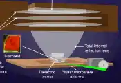
At the heart of the effort were Fermilab-developed cryoelectronics — specialized circuits designed to operate at the extreme cold temperatures required for quantum computers. These cryoelectronics were integrated into MIT Lincoln Laboratory’s ion-trap platform to test whether they could reliably perform key functions: moving individual ions, holding them at set positions and measuring the effects of electronic noise.
Why ion traps?
Ion-trap quantum computers use charged atoms confined by electric or magnetic fields as qubits. Such systems are prized for their long coherence times and high-fidelity operations.
However, scaling them to millions of qubits, as needed for advanced applications, is a major challenge. Today’s systems rely on lasers and extensive wiring between room-temperature electronics and cryogenic ion traps — a setup that becomes increasingly impractical as the number of ions grows.
By placing ultra-low-power cryoelectronics near the ion traps, the Fermilab–MIT Lincoln Laboratory team realized a promising path forward. Their redesigned system replaced some of the room-temperature controls with a chip mounted inside the cryogenic environment. The researchers successfully demonstrated this hybrid approach could move and control ions.
“In addition to demonstrating feasibility, we learned a lot,” said Farah Fahim, head of Fermilab’s Microelectronics Division. “By showing that low-power cryoelectronics can work inside ion-trap systems, we may be able to accelerate the timeline for scaling quantum computers, bringing closer into reach what seemed decades away. This approach could ultimately support systems with tens of thousands of electrodes or more.”
Future work will directly connect the electronics with the ion-trap chips, further increasing efficiency and performance and enabling scaling of ion-trap arrays for larger systems.
Lessons learned
The experiment also surfaced new insights that will guide future chip designs. For instance, transistors that behaved well in Fermilab’s setup did not perform as well in MIT Lincoln Laboratory’s significantly colder environment, impacting the control circuit performance and operation range.
Also, the circuits initially held voltages for milliseconds. Though modifications extended the hold times, further modifications will be required to further extend them to the minutes or hours large systems require. Addressing these and other challenges will be central to the next round of development.
Robert McConnell, a technical staff member at MIT Lincoln Laboratory, said that “while there are still significant challenges to establishing the technology needed to control ion arrays of a practical scale, this demonstration of small-form-factor, low-noise electronics lays the foundation for hybrid-integrated systems we hope to develop in the near future.”
The successful integration highlights the value of cross-center collaboration, in addition to marking a concrete step toward realizing scalable quantum computing technologies for science and beyond.
Topics:
Most Recent


NewsFlash
Industry Pioneers
Editor's Picks
-

IBM to Acquire HRL Laboratories to Power the Future of Quantum
-

PsiQuantum Signs $125 Million Agreement With DARPA
-

Trump Administration Announces More Than $5 Billion for the Genesis Mission, a National Mission on AI for Science
-

Infleqtion to Deploy Fault-Tolerant Neutral-Atom Quantum Computer in Illinois