Vexlum Raises EUR 10 Million to Scale Semiconductor and Laser Manufacturing to Meet Global Demand
TAMPERE, Finland, February 05, 2026 -- Vexlum, a manufacturer of advanced semiconductor lasers for high-impact applications, has announced it has secured EUR 10 million in funding to scale its proprietary semiconductor chip manufacturing and laser technology operations in Finland. The round consists of EUR 6 million in equity investment led by Kvanted, with participation from Finnish state-owned Tesi (Finnish Industry Investment Ltd) and the EIC Fund, alongside a EUR 2.4 million grant from the EIC Accelerator, and a EUR 1.6 million loan from Nordea.
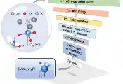
Vexlum’s semiconductor-based Vertical-External-Cavity Surface-Emitting Laser (VECSEL) technology addresses a critical bottleneck in high-tech industries: the lack of compact, cost-effective, high-power laser sources at precise wavelengths. Applications, such as atomic clocks and quantum computers, as well as next-generation semiconductor metrology and free-space optical communication technology, all rely heavily on lasers.
Now, Vexlum is expanding its manufacturing capabilities in Finland to ensure quality and speed as the company responds to strong market demand following the introduction of several product lines.
“Securing and scaling our semiconductor fabrication infrastructure is critical for the market’s evolution. It allows us to ensure that the laser quality and reliability meet our customers’ stringent requirements,” said Jussi-Pekka Penttinen, CEO and Co-founder of Vexlum. “We are moving beyond boutique production to industrial-scale capability. This funding allows us to bring our semiconductor manufacturing into a new, expanded facility here in Tampere and scale our capacity to meet the demand from the quantum, semiconductor, and space sectors.”
The fabrication of Vexlum’s chips starts with molecular beam epitaxy, where the semiconductor wafer is “grown” in a reactor, atomic layer by atomiclayer – akin to 3D printing on an atomic scale.
Unlike the silicon used in traditional electronics, Vexlum utilizes III-V semiconductor materials (such as gallium arsenide, indium phosphide, and gallium antimonide) to produce laser wafers for specific wavelengths. The wafers are fabricated into laser chips in a specialized cleanroom, after which the quality-controlled, ready chips are integrated into laser systems to generate laser light. This vertical integration in a facility owned by Vexlum allows the company to control the entire value chain – from chip manufacturing to the final laser system – and to address customer needs.
“Tampere has emerged as a leading hub for optoelectronics and III-V semiconductor technology, building on a strong foundation of world-class academic research and a proven ability to translate it into industrial innovation. This investment round represents a decisive step in scaling our ambitions, securing a leading position for Tampere and Finland in the advanced semiconductor industry,” said Mircea Guina, Chairman and Co-Founder of Vexlum.
The financing represents a significant milestone for the Nordic deep tech ecosystem, standing as potentially the largest seed round ever raised by a photonics company in the region. The funding will drive Vexlum’s growth strategy, which is aiming for EUR 100 million in revenue by 2030.
Kvanted, a Nordic venture capital firm focused on industrial technology, sees Vexlum as a prime example of the Tampere region’s deep-tech engineering prowess in laser technology.
“We are not just investing in a laser company. Instead, we are investing in a semiconductor manufacturer that has cracked the code on scaling high-power, precise wavelengths for the world’s most difficult problems. Our fund is proud to back a team that is turning this know-how into a global category leader,” said Axel Ahlström, Founding Partner at Kvanted.
Currently a major supplier for trapped-ion quantum computers, Vexlum’s ability to manufacture lasers across diverse wavelengths allows the company to power solutions far beyond quantum labs. For example, the technology is also being developed to make satellite optical communications more reliable, to enable next-generation optical atomic clocks that aim to redefine the precision of timekeeping, and for other uses where specific laser colors are needed.
“The quantum ecosystem has taught us that extreme precision is only valuable if it can be delivered reliably and at scale. We are now taking those hard-won lessons and applying them to the broader photonics landscape,” said Jussi-Pekka Penttinen. “Whether for satellite communications or semiconductor metrology, we are proving that the rigorous architecture developed for quantum computers is the same engine needed to drive the next generation of industrial innovation.”
Topics:
Most Recent


NewsFlash
Industry Pioneers
Editor's Picks
-

Four Leading Quantum Companies Sign-On to ABQ-Net, the First Open-Access Quantum Network in the United States
-

Multiverse Computing Announces Series C Fundraising Targeting Up to $570M (€500M) to Power Efficient AI From Edge to Cloud
-
NRL Advances the Navy’s Quantum Future as America Accelerates Quantum Innovation
-
SKKU Identifies World’s First ‘Zinc Oxide Spin Qubit’ — a Breakthrough for Semiconductor-Based Quantum Technology