Scientists Reveal Hidden Interface in Superconducting Qubit Material
UPTON, N.Y., May 05 2025 -- Researchers from the U.S. Department of Energy’s (DOE) Brookhaven National Laboratory and DOE’s Pacific Northwest National Laboratory (PNNL) have uncovered an unexpected interface layer that may be hindering the performance of superconducting qubits, the building blocks of quantum computers. While examining this layer through a combination of imaging techniques and theoretical models, they discovered the underlying cause of puzzling structural differences in qubits.
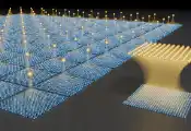
The unexpected layer is called a metal-substrate interface, or M-S interface, because it lies between a layer of tantalum metal and a sapphire substrate. Researchers from the Co-design Center for Quantum Advantage (C2QA), a DOE National Quantum Information Science Research Center led by Brookhaven Lab, have fabricated high-performing superconducting qubits made up of a tantalum thin film deposited on a sapphire substrate. But to unlock the potential power of quantum computers, qubits must exhibit a higher “coherence time,” meaning they need to retain quantum information for longer.
Quantum researchers have dedicated significant efforts to determining which constituent materials and fabrication techniques yield qubits with the highest coherence times. But there are several other elements of qubit architecture that could also affect coherence times. For example, when a qubit is exposed to air, the surface-level tantalum reacts with oxygen. This results in a tantalum oxide layer on the surface of the qubit, and C2QA researchers have found that the interface between this oxide layer and the tantalum thin film hinders the qubit performance. They’ve even explored coating tantalum to prevent the oxidation from occurring.
“We knew that the interface between tantalum oxide and tantalum had a pretty big effect on the performance of qubits made with tantalum thin films,” explained Aswin kumar Anbalagan, a researcher at the National Synchrotron Light Source II (NSLS-II) and first author on the recent Advanced Science publication. “That led us to question whether the other interface, the one between the tantalum and the sapphire, was also affecting qubit performance.”
Thinner samples, deeper insights: probing the M-S interface
The high-performing superconducting qubits fabricated by C2QA researchers are typically between 150 and 200 nanometers thick. Though they are incredibly thin — for context, a human hair is 80,000-100,000 nanometers wide — they are too thick to characterize with certain X-ray techniques.
Anbalagan and his mentors at NSLS-II wanted to explore the region where the tantalum metal meets the sapphire substrate, so they partnered with researchers from the Center for Functional Nanomaterials (CFN) to fabricate thinner samples — around 30 nanometers thick — made from the same materials as traditional qubits.
“At CFN, we have developed a technique to fabricate high-quality tantalum thin films for quantum circuitry applications,” said Mingzhao Liu, senior scientist at CFN and co-author on the paper. “In this case, we adopted the same technique to fabricate tantalum films that are much thinner, with a very smooth surface and interface against sapphire.” NSLS-II and CFN are DOE Office of Science user facilities at Brookhaven Lab.
“We started with some reasonably straightforward measurements at NSLS-II to see the interface below the tantalum thin film,” said Andrew L. Walter, a lead beamline scientist in NSLS-II’s electronic structure techniques program and one of the lead authors on the paper.
The researchers conducted X-ray reflectivity experiments at the Beamline for Materials Measurement (BMM). These studies offered insights into the thickness and density of each layer in the sample. They also leveraged the Spectroscopy Soft and Tender 2 (SST-2) beamline to take X-ray spectroscopy measurements that revealed the chemical makeup of the layers. The BMM and SST-2 beamlines at NSLS-II are funded and operated by the National Institute of Standards and Technology (NIST).
“We were expecting to see a clean interface between the tantalum and the substrate,” Walter said. “But our measurement showed that something more interesting was going on at the interface.”
The researchers’ measurements at BMM revealed a previously unobserved, buried layer between the tantalum metal and the sapphire substrate.
“We tried to explain the data many other ways, but the thin layer at the interface was the only way to resolve our unexpected result,” said Andi M. Barbour, beamline scientist at NSLS-II and co-lead author on the paper.
Anbalagan added, “If we had observed a layer this thin in a sample that was 150 nanometers thick, it probably would not have captured our attention in the same way. This work would not have been possible without the thin samples, but that was just the start of this project. Our colleagues were skeptical about the complexities of the M-S interface, but we convinced them to take more sophisticated and time-intensive measurements so we could take a closer look.”
C2QA researchers from Brookhaven’s Condensed Matter Physics and Materials Science (CMPMS) Department found a layer of tantalum atoms intermixed with aluminum and oxygen atoms from the sapphire substrate using scanning transmission electron microscopy (STEM) and electron energy-loss spectroscopy (EELS).
These techniques complemented the studies conducted at NSLS-II as their high spatial resolution uniquely suits them for probing the interfaces of thin layers.
“STEM and EELS not only enable direct observation of atomic arrangement at the interface but also reveal their electronic bonding states,” said Yimei Zhu, a co-author of the paper from CMPMS.
Consistent with prior research, the experimentalists also observed different orientations of the tantalum thin film deposited on the sapphire.
“It’s like cutting a cake from different orientations,” explained Barbour. “The way a cake is typically cut, you can see layers of cake and icing. But if you rotate the cake on its side, you may see only cake or only icing in the cross-section. In this scenario, the crystallographic structure of the tantalum atoms is like the cake and icing.”
Computational collaborations
Across the country, PNNL materials scientist and paper co-lead author Peter V. Sushko used computational techniques to help determine why there were two different tantalum orientations — and sometimes a mixture of the two orientations — at the M-S interface.
“This question is easier to address with computational work, rather than an experiment, because computationally I can control the positions and concentrations of atoms with what feels like a ‘magic hand,’” Sushko explained.
Modeling like this offers insights into how different material properties are determined by atomic-scale interactions, and Sushko found that oxygen concentration at the sapphire substrate’s surface plays a significant role in the direction of tantalum’s deposition. In other words, if the substrate has a high concentration of oxygen at its surface, the tantalum deposits in one orientation. If there is a low oxygen concentration at the sapphire’s surface, the tantalum deposits in the other orientation.
“There’s quite remarkable agreement between Peter’s calculations and the transmission electron microscopy measurements,” said Walter. “I don’t see such good correlations very often.”
Barbour added, “We knew that something at this interface played a role in degrading qubit performance, but we had no idea the oxygen concentration at the substrate’s surface could have such drastic effects. Our experimental data would not have had nearly the same impact without Peter’s contributions.”
Path forward
With a better understanding of what causes the different tantalum orientations, researchers will now be able to adjust different aspects of qubit fabrication to control the amount of oxygen at the substrate’s surface and, consequently, the orientation of tantalum’s deposition. Though they do not yet know which orientation — or combination of orientations — optimizes qubit performance, this is one direction for future research.
“This work shows how X-ray reflectivity measurements might be a powerful tool in prototyping or figuring out how you want to grow your samples,” said Barbour, referring to how the hours-long X-ray characterizations informed and motivated the more complex and labor-intensive STEM experiments. “X-ray reflectivity can be a quick and effective way to start to understand the impacts of different fabrication techniques.”
Furthermore, tests conducted by Brookhaven physicists confirmed that the proxy sample used in this research exhibited superconducting properties required for functional qubits, opening the door to potentially reducing qubit size in the future.
From the experimentalists using state-of-the art instrumentation on the East Coast of the United States to theorists employing cutting-edge computational techniques on the West Coast, this project incorporated a breadth of expertise and tools — and spanned a continent. But it would not have been possible without the interdisciplinary and cross-institutional structure of C2QA.
“It really takes a lot of different scientists with different backgrounds to progress towards building better qubits,” said Barbour. “A core aim of C2QA is getting all the right groups of people together, and this work is just one part of the Center’s many contributions to quantum computing.”
Brookhaven National Laboratory is supported by the Office of Science of the U.S. Department of Energy. The Office of Science is the single largest supporter of basic research in the physical sciences in the United States and is working to address some of the most pressing challenges of our time.
Most Recent


NewsFlash
Industry Pioneers
Editor's Picks
-

Infleqtion to Deploy Fault-Tolerant Neutral-Atom Quantum Computer in Illinois
-

Start of IBERIANQCI, the Quantum Communications Infrastructure of the EuroQCI Program for Spain and Portugal
-

NIS 100 Million to Establish a National Quantum Computing R&D Infrastructure
-

OptQC and AIST Commence Initial Operations of "MoQuren," OptQC's First Optical Quantum Computer