Building Quantum Computers With Leading-Edge Semiconductor Fab
November 12, 2025 -- Building quantum computers at scale means treating quantum chips like the state-of-the-art hardware that they are. It means fabricating them to the highest standards of quality—similar to the standards they use to fabricate chips for production-scale classical computers.
Today, IBM has revealed that IBM Quantum Loon and IBM Quantum Nighthawk—plus all future chips on the IBM Quantum Development Roadmap—are being fabricated at NY CREATES' Albany NanoTech Complex using state-of-the-art 300mm semiconductor wafer technology. The Albany NanoTech Complex is one of the world’s most advanced semiconductor fabs and the details of their quantum chip fab processes have been held under wraps to this point. But now, the team is eager to show off the technology, share how they pulled the project off, and deliver their vision for the future.
This story is about more than processing quantum chips on larger wafers. It’s about using the best possible minds, machinery, and processes to realize quantum computing. The fabrication of IBM Quantum chips at the Albany NanoTech Complex—and the close synchronization between semiconductor experts and physicists across Albany and at the IBM Thomas J. Watson Research Center in Yorktown—is key to the success of quantum computing at IBM.
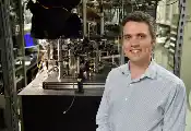
“If we had not started processing our chips at Albany using 300mm technology, we wouldn’t have achieved the success required to pull off our development roadmap,” said Christy Tyberg, Distinguished Engineer of Quantum Fab Technology & Infrastructure at IBM.
Fabricating chips—quantum or classical
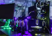
The processors at the heart of IBM quantum computers are crafted the same way classical computer chips are: from silicon wafers. The semiconductor fabrication process begins with long cylinders of silicon sliced into thin disks. Engineers and physicists use computer software to design electrical circuits. Then—through a series of process steps—automated machines etch, deposit new metals, and treat the wafers. The result is a rectangular grid of computer chips on the surface of the disk.
In the case of quantum chips, they fabricate multiple wafer types, and then complete additional custom processing steps at Yorktown. Finally, they layer and connect multiple chips in a 3D stack, and hook them up to the control electronics.
Whether quantum or classical, computer chips require the most precise manufacturing and clean-room conditions. Any particles or defects can impact performance, given the microscopic size of classical computer transistors and the ultra-sensitive nature of quantum bits.
What does wafer size mean? At the most general level, the wafer’s width governs how many chips it will yield. Wafer size has increased incrementally during the 20th century, and the early 90s introduced the 200mm wafer—about 8 inches. Smaller-scale semiconductor fabs process wafers measuring 200mm or smaller. However, the turn of the century brought 300mm wafers—around 12 inches.
Each technology comes with a different set of tooling. 300mm features state-of-the-art tools and processes for fabricating more chips, faster. Meanwhile, 200mm allows for more hands-on, custom R&D.
When Tyberg joined IBM in 2000, she started researching semiconductors, specifically materials called low-κ dielectric materials, followed by process development for 3D chip stacking technology intended to help continue Moore’s law. It wasn’t until 2016 that she was asked whether she wanted to move to quantum computing. She figured quantum was a long ways away—IBM was only just starting to put small, experimental systems on the cloud. But she thought the project sounded exciting and joined the team.
Tyberg began with the basics, learning what quantum computing was and how her semiconductor experience could advance the technology. Today, she focuses on developing the processes that achieve the long-term objective of realizing quantum computing as a full-scale production compute system.
Those first chips were built at the 200mm research-scale fabrication laboratory at IBM Research in Yorktown Heights, and required specialized tools and processes. Fabricating wafers with quantum chips was a bespoke endeavor, and building new tools, processing, troubleshooting, and fixing problems took a long time. Processing happened 5 days a week in two shifts.
In 2021, Tyberg and Jay Gambetta, now director of IBM Research, discussed what it would take to treat quantum as a production technology using the 24/7 300mm fab available to them. For near-term quantum computing, an ideal process would be one that could be partially automated using state-of-the-art 300mm technology, while still relying on 200mm for custom or especially challenging process steps.
Quantum goes to Albany
The Albany NanoTech Complex is a unique public-private partnership that began in 2002 when IBM, Tokyo Electron, and New York State came together at the campus of State University of New York to build the most advanced semiconductor R&D facility in the country. Today, IBM continues to be an anchor partner of the cutting-edge facility, and over the last two decades Albany NanoTech has become the most successful ecosystem for semiconductors, attracting more than $20B in investment.
Leveraging state-of-the-art equipment and decades of expertise, IBM Research Albany continues to pioneer breakthroughs in materials science, nanotechnology, and chip design. This includes the research and development of nanosheet technology that would allow IBM to deliver the world’s first 2nm chips. It only made sense that Albany would be a part of the mission to build the future of quantum computing.
“We became the accelerator for IBM’s quantum hardware mission and roadmap,” said Hemanth Jagannathan, Distinguished Engineer and Director responsible for Process Technology R&D and Semiconductor Acceleration for Quantum at IBM Research. “There were needs articulated by the quantum team and we would understand them, figure out the processes involved, the integration involved, and how to build the devices with speed and at scale.”
Jagannathan joined IBM in 2006 researching novel materials and processes to advance the scaling of digital electronics, specifically on high-k dielectrics and metal gate technology. Over the years he has driven a variety of innovations pushing IBM’s advanced logic roadmap forward. He was also the technical executive responsible for Chiplet and Advanced Packaging Technology, driving solutions for the IBM’s AI hardware roadmap.
As a veteran in semiconductor materials, process, device architectures and packaging technology, Jagannathan was asked to be a lead on the project when the quantum team came to Albany in 2021. His broad, deep knowledge made him a logical fit for the quantum project. He’d be leading a team tasked with process development and integration for quantum processor wafers.
But quantum wasn’t like classical. Despite the name, qubits, essentially the transistors of the quantum chip, are very different from the 2nm nodes designed for classical chips. They couldn’t use textbook processes. Everything the quantum team asked for would be different—different materials, different tools, components arranged and wired in entirely new ways.
Perhaps the biggest difference would be the time. Whereas classical semiconductor teams might have a few years to create and perfect chips, IBM Quantum had published a bold roadmap, committing to new chips annually that would scale in both size and performance, with a promise for a fault-tolerant quantum computer by 2029.
The joint quantum-semiconductor team would need to write the rules for quantum chip production in the same way that engineers in the 70s and 80s wrote the rules for bipolar junction transistors (BJTs) and metal oxide semiconductor field effect transistors (MOSFETs). And they’d need to figure things out in just a few years. This required a new way of doing R&D.
Building a culture of learning at speed
Tyberg and Jagannathan began building out a tightly linked joint team tasked with realizing quantum chips across Albany and Yorktown.
First, physicists partner with fabrication engineers to dream up designs for a chip capable of delivering the scale, quality, and speed required to advance quantum computing. These designs are then released to the fabrication team, which is tasked with turning the ideas into processes that can be undertaken and repeated on real 300mm wafers.
In the near term, some of those wafers are then cored to 200mm, where additional custom processes can be completed. The wafers go through additional final assembly and then into dilution fridges so physicists can ensure that they work.
Quantum technology poses new challenges to chip design and fabrication engineers. Qubits can have unwanted interactions with one another and cause errors, so they needed a component that could shut off qubit-to-qubit interactions. They needed to be able to control multiple qubits with the multiple sets of wires, and have wires cross over and under one another. And with the most recent chip, they needed to connect qubits beyond just nearest neighbors, but the team required help on the semiconductor side to figure it all out.
The ever-growing team began building a collaborative and high-performance culture tasked with solving these problems. It wouldn’t be a one-way conversation of physicists making requests and process technologists solving them. Physicists and process integrators spoke often to understand the problems together. And the team worked ‘round the clock to keep to quantum’s tight deadlines.
An official unmasking
A strong foundation in semiconductor technology development and access to 300mm fab facilities have played a key role in cementing IBM's quantum computing leadership. With the capabilities and capacity of the 300mm fab, researchers can explore a greater variety of chip designs in significantly less time. Albany NanoTech processes wafers 24 hours a day, 7 days a week. As a result, they are able to reduce cycle times significantly. This allows researchers to iterate and implement improvements in quick cycles of learning.
But the true key to success is that the team has created a tightly coupled process across the Albany and Yorktown locations that allows them to reap the benefits of state-of-the-art 300mm technology, established 200mm processes, and expertise across both paradigms to develop chips like Heron, Nighthawk, and Loon on schedule. Replicating and innovating the process steps to make qubits with millisecond coherence times on these wafers is a true testament to what they can achieve when teams work together.
“IBM is in a very unique position as a company that has internal access to both 200 and 300mm fabs,” said Tyberg. “It really gives us an advantage if we fully take advantage of those capabilities.
With the first waves of Nighthawk and Loon out of the fab, the joint team can take some time to celebrate with an event featuring lots of cake and a room filled with swag related to the specific bird. Still with Kookaburra, Cockatoo, Starling, and Blue Jay on the horizon, the journey is only just beginning. There’ll be many all-new challenges to solve. But the team is feeling confident.
“There is a lot of rapid innovation and maturity which has to happen over the next few years to deliver these systems. But the raw talent and expertise that goes into every aspect of what we're building—not only in semiconductors, but also by the team building the systems—these are experts working at levels which are probably unimaginable to the outside world to build the systems which we build," said Jagannathan. “I may be biased, but I'm very, very bullish in saying that we are probably the only company on the planet that can do this."
“There is a lot of rapid innovation and maturity which has to happen over the next few years to deliver these systems. But the raw talent and expertise that goes into every aspect of what we're building—not only in semiconductors, but also by the team building the systems—these are experts working at levels which are probably unimaginable to the outside world to build the systems which we build," said Jagannathan. “I may be biased, but I'm very, very bullish in saying that we are probably the only company on the planet that can do this."
Topics:
Most Recent


NewsFlash
Industry Pioneers
Editor's Picks
-
NRL Advances the Navy’s Quantum Future as America Accelerates Quantum Innovation
-
SKKU Identifies World’s First ‘Zinc Oxide Spin Qubit’ — a Breakthrough for Semiconductor-Based Quantum Technology
-

EuroHPC JU Launches Procurement for a Quantum Computer in Luxembourg
-

IBM to Acquire HRL Laboratories to Power the Future of Quantum