memQ Delivers Integration of Advanced Quantum Computing Components with Commercial Foundry Processes
CHICAGO, IL, July 31, 2025 memQ™, the industry leader in quantum networking solutions for distributed quantum computing, today announced breakthrough technology and processes that allow scalable and cost-effective production of quantum networking components using common semiconductor production capabilities. This approach, now used in their xQNA quantum memory modules, has been demonstrated as compatible with large-scale 300 mm silicon wafer processing to deliver truly scalable single photon sources supporting the ubiquitous telecom C-band. See the full peer reviewed work in Nanoletters.
The past year has seen technological breakthroughs from major technology players including AWS, Google, IBM, and Microsoft, coupled with significant venture investment in the quantum computing sector; over $1.25B was invested in pure-play quantum technology companies in the first quarter of 2025 alone. A key obstacle in bringing these innovative solutions to market has been the requirement to develop and implement new manufacturing techniques which can support commercial production of these new ultra-demanding new technologies in a replicable, high-yield manner. The memQ approach is unique in its ability to blend the science of quantum technologies with proven, existing semiconductor manufacturing processes in a way that delivers reliable production at scale.
“Our work leverages advanced silicon photonics to create a manufacturable, C-band compatible quantum memory platform using today’s reliable processes in a way that delivers cavity performance and uniformity exceeding that which can be achieved through chip-scale e-beam lithography,” stated Manish Kumar Singh, memQ CEO. “Not only is this key in enabling us to reliably produce cost-effective quantum memory at scale but also provides a path for working with commercial foundries known for their strict material and process controls that are often prohibitive for novel materials.”
The tapeout of the wafer was performed under CRADA with the Air Force Research Lab (AFRL), Rome New York and performed by AIM Photonics through the shared foundry facility at NY CREATES’ NanoTech Complex in Albany, New York.
“The Air Force Research Laboratory is dedicated to ongoing research aimed at utilizing quantum channels across various distances,” remarked Michael Hayduk, Deputy Director of the AFRL Information Directorate. “Our partnerships with industry collaborators play a vital role in our commitment to advancing the scale and maturity of advanced photonics integration in a timely manner.”
These developments also illustrate the potential for traditional photonics industry players to become involved in the quantum market by demonstrating how typical photonic control components, such as high quality/low mode volume photonic crystal cavities, can be reliably produced on proven 300 mm wafer processes. This capability will be integral to implementing quantum networking architectures that can preserve the quantum state both locally and at a distance.
“In addition, a positive side-effect is that components developed by memQ in AIM Photonics’ 300 mm QFlex technology, will be available to PDK users strengthening the Institute’s mission of promoting the silicon photonics industrial base in the U.S.,” adds Gerald (Jerry) L. Leake, Sr. Research Engineer at AIM Photonics.
“At GQI, we have long held that in order for quantum to reach commercial advantage it must demonstrate that it can be produced reliably, at scale, and without massive investment in new factories,” said Andre Konig, CEO of Global Quantum Intelligence. “memQ offers a powerful demonstration of how monolithic integration of novel materials, such as their Erbium-doped TiO2 qubits, can be readily achieved on today’s foundry platforms, opening the door for a broader merging of quantum and commercial photonics.”
In addition to this published work, memQ has recently released a new paper on arXiv that uses this approach to demonstrate monolithic integration of solid-state quantum memories with commercial foundry photonics using back-end-of-line (BEOL) deposition. This is a crucial step towards scalable quantum interconnects. We utilized erbium-doped titanium dioxide (Er:TiO2) thin films on silicon nitride waveguides. The platform demonstrates exceptional optical coherence (64 µs), second-long electron spin lifetimes, and electrical control of Er emission. This establishes Er:TiO2 on foundry photonics as a manufacturable platform for both ensemble and single-ion quantum memories, paving the way for high-efficiency quantum networking.
Topics:
Most Recent


NewsFlash
Industry Pioneers
Editor's Picks
-

European Consortium QUARTERNEXT Launches to Advance Next-Generation Quantum-Safe Communications for Industrial Deployment and Certification
-

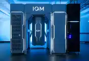
IQM Selected to Deliver the LUMI-IQ Quantum Computer
-

NSF Launches Project Triad to Advance Quantum Technology for Real-World Applications
-

A New Ultra-Compact Sensor Paves the Way for More Powerful and Scalable Silicon Quantum Processors