Aeluma and Thorlabs Unveil Breakthrough With Large-Diameter Wafer Manufacturing Platform for Quantum Computing and Communication
GOLETA, CA, May 29 2025 -- Aeluma, Inc., a semiconductor company specializing in high-performance, scalable technologies, together with Thorlabs, a vertically integrated photonics products manufacturer, today announced a major advancement in silicon photonics that could accelerate adoption of quantum computing and communication at commercial scale.
Aeluma's large-diameter wafer platform combines the performance of compound semiconductors with the scale of mainstream silicon manufacturing, enabling cost-effective solutions across high-growth markets including mobile, AI, defense and aerospace, automotive, and quantum computing.
Silicon photonics is a promising technology for quantum computing and communication. Aeluma's ability to incorporate quantum dot sources and highly nonlinear electro-optic materials unlocks new high-performance functionality for this platform.
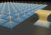
Collaborating with Thorlabs, and with support from the Office of Secretary of Defense, Aeluma successfully demonstrated wafer-scale integration of aluminum gallium arsenide, a nonlinear optical material, onto CMOS silicon photonics standard 200mm diameter wafers, providing a path for scaling complex quantum photonic circuits.
The nonlinear optical material enables entangled photon pair generation and modulation, key building blocks for quantum photonic systems. Compared with other materials like silicon nitride or lithium niobate, aluminum gallium arsenide offers significantly improved efficiency for next-generation quantum photonic circuits.
"Scalable photonic integration is essential to move quantum technologies out of the lab and into real-world systems," said Matthew Dummer, Ph.D., Director of Technology at Aeluma. "By merging the performance of compound semiconductors with the scalability of silicon photonics, we are pushing the boundaries of what's possible in quantum and AI."
This combination of advanced materials and CMOS silicon substrates, using manufacturing methods compatible with mainstream fabs, marks a step toward volume production, which could move quantum technologies out of research labs and into mass-market products.
"This successful collaboration was enabled by the large-area epitaxial growth capabilities of Aeluma and the direct wafer bonding expertise at Thorlabs," added Garrett Cole, Ph.D., Manager of Thorlabs Crystalline Solutions. "The heterogeneous integration of compound semiconductor materials on silicon is broadly applicable and now shows significant promise for quantum photonics."
The breakthrough demonstration complements Aeluma's work with quantum dot materials in 300mm silicon photonics, aimed at optical interconnects for AI infrastructure and advanced sensing. It directly addresses a longstanding challenge in scaling quantum photonic systems and could provide a meaningful step forward for quantum system integrators pursuing scalable, production-ready solutions.


