Engineering Quantum Entanglement at the Nanoscale
January 13, 2025 -- Physicists have spent more than a century measuring and making sense of the strange ways that photons, electrons, and other subatomic particles interact at extremely small scales. Engineers have spent decades figuring out how to take advantage of these phenomena to create new technologies.
In one such phenomenon, called quantum entanglement, pairs of photons become interconnected in such a way that the state of one photon instantly changes to match the state of its paired photon, no matter how far apart they are.
Nearly 80 years ago, Albert Einstein referred to this phenomenon as "spooky action at a distance." Today, entanglement is the subject of research programs across the world — and it’s becoming a favored way to implement the most fundamental form of quantum information, the qubit.
Currently, the most efficient way to create photon pairs requires sending lightwaves through a crystal large enough to see without a microscope. In a paper published today in Nature Photonics, a team led by Columbia Engineering researchers and collaborators, describe a new method for creating these photon pairs that achieves higher performance on a much smaller device using less energy. P. James Schuck, associate professor of mechanical engineering at Columbia Engineering, helped lead the research team.
These findings represent a significant step forward in the field of nonlinear optics, which is concerned with using technologies to change the properties of light for applications including lasers, telecommunications, and laboratory equipment.
“This work represents the embodiment of the long-sought goal of bridging macroscopic and microscopic nonlinear and quantum optics,” says Schuck, who co-directs Columbia's MS in Quantum Science and Technology. “It provides the foundation for scalable, highly efficient on-chip integrable devices such as tunable microscopic entangled-photon-pair generators.”
How it works
Measuring just 3.4 micrometers thick, the new device points to a future where this important component of many quantum systems can fit onto a silicon chip. This change would enable significant gains in the energy efficiency and overall technical capabilities of quantum devices.
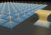
To create the device, the researchers used thin crystals of a so-called van der Waals semiconducting transition metal called molybdenum disulfide. Then they layered six of these crystal pieces into a stack, with each piece rotated 180 degrees relative to the crystal slabs above and below. As light travels through this stack, a phenomenon called quasi-phase-matching manipulates properties of the light, enabling the creation of paired photons.
This paper represents the first time that quasi-phase-matching in any van der Waals material has been used to generate photon pairs at wavelengths that are useful for telecommunications. The technique is significantly more efficient than previous methods and far less prone to error.
“We believe this breakthrough will establish van der Waals materials as the core of next-generation nonlinear and quantum photonic architectures, with them being ideal candidates for enabling all future on-chip technologies and replacing current bulk and periodically poled crystals,” Schuck says.
“These innovations will have an immediate impact in diverse areas including satellite-based distribution and mobile phone quantum communication.”
How it happened
Schuck and his team built on their previous work to develop the new device. In 2022, the group demonstrated that materials like molybdenum disulfide possess useful properties for nonlinear optics — but performance was limited by the tendency of light waves to interfere with one another while traveling through this material.
The team turned to a technique called periodic poling to counteract this problem, which is known as phase matching. By alternating the direction of the slabs in the stack, the device manipulates light in a way that enables photon pair generation at miniscule length scales.
“Once we understood how amazing this material was, we knew we had to pursue the periodic poling, which could allow for the highly efficient generation of photon pairs,” Schuck says.
This work occurred within Programmable Quantum Materials, a Department of Energy energy frontier research center (EFRC) at Columbia, as part of a larger effort to understand and exploit quantum materials. This work was possible due to contributions from the Baso, Delor, and Dean labs. Postdoctoral researcher Chiara Trovatello led the effort.

