Development of Ultra-Fast Quantum Tunneling Device for 6G Terahertz Era
January 09, 2026 -- A research team, affiliated with UNIST has unveiled a groundbreaking quantum device, capable of ultra-fast operation, a key step toward realizing technologies like 6G communications. This innovation overcomes a major hurdle that has long limited the durability of such devices under high electric fields.
Professor Hyeong-Ryeol Park from the Department of Physics at UNIST, in collaboration with Professor Sang Woon Lee at Ajou University announced the successfully development of a terahertz quantum device that can operate reliably without suffering damage from intense electric fields—something that has been a challenge for existing technologies.
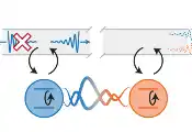
Terahertz quantum devices are considered essential for future high-speed communication systems, enabling rapid signal processing well beyond the limits of traditional semiconductors. They work by harnessing the quantum tunneling of electrons driven by terahertz waves—high-frequency electromagnetic waves oscillating billions of times per second—a phenomenon where electrons pass through energy barriers in a way classical physics can’t explain.
The main obstacle has been that inducing tunneling requires extremely strong electric fields—around 3 volts per nanometer—which generate a lot of heat. This heat often damages or melts the device’s metal electrodes, making reliable operation difficult.
To tackle this, the team developed a new device that can operate at much lower electric fields—roughly a quarter of what was previously needed. The secret lies in replacing the insulator material sandwiched between the metal electrodes. Instead of using the conventional aluminum oxide (Al₂O₃), they used titanium dioxide (TiO₂), which has a lower energy barrier and allows electrons to tunnel with less effort.
Gangseon Ji, the first author of the study, explained, “Rather than pushing electrons with stronger electric fields, we’re creating pathways that make it easier for electrons to move. Since tunneling is a probabilistic quantum effect, lowering the energy barrier significantly increases the chances of tunneling happening.”
Using advanced atomic layer deposition techniques, the team produced high-quality devices. This method, commonly used in semiconductor manufacturing, allowed precise control over the TiO₂ layer, preventing microscopic defects—such as oxygen vacancies—that often occur during thin-film fabrication.
Professor Lee added, “By applying cutting-edge deposition technology, we managed to eliminate defects that could weaken the device, ensuring high stability and performance.”
The new device demonstrated consistent tunneling operation at electric fields of about 0.75 V/nm. Thanks to TiO₂’s excellent thermal properties, it maintained stable performance over 1,000 cycles, even when modulating terahertz wave transmission by up to 60%. This level of stability was a significant achievement, pointing toward practical applications.
Professor Park concluded, “We have addressed the two biggest challenges—high-voltage operation and heat-related damage—that have held back the commercialization of terahertz quantum devices. This breakthrough opens the door to ultra-fast, energy-efficient optical communication systems beyond 6G and advanced quantum sensing technologies.”
The findings of this research have been published in the online version of ACS Nano on December 20, 2025. The project was supported by the National Research Foundation of Korea (NRF) and the Institute of Information & Communications Technology Planning & Evaluation (IITP), among others.
Topics:
Most Recent


NewsFlash
Industry Pioneers
Editor's Picks
-

Honeywell Aerospace-Led Consortium to Develop Compact Quantum Space Magnetometer to Advance Research Into Earth’s Magnetic Field
-

European Quantum Communication Infrastructure: Deutsche Telekom and AIT Will Coordinate PETRUS2 and HarmoniQCI
-

Quantinuum, Rolls-Royce, Riverlane and University of Edinburgh Sign Agreement to Explore Quantum Computing for Industrial Design and Simulation
-

World’s First Superconducting Quantum Heat Engine Opens the Path to Larger Quantum Computers