Stefan Strauf’s Research Brings Virtually Unhackable Free-Space Quantum Communication One Step Closer to Reality
April 10, 2025 -- ACS Nano features the physics professor’s latest breakthrough, developing an advanced, scalable method for creating, brightening and directing light on a chip for quantum cryptography and photon-encrypted telecommunications of the future.
Free-space quantum communication uses particles of light called photons to transfer data through the Earth’s atmosphere and nearby space. Still in its infancy, this technology holds the potential to transmit sensitive information — from bank transactions to critical infrastructure operations — far more securely than is possible through current classical communication methods. Rather than relying on man-made algorithms, quantum communications use the fundamental principles of quantum mechanics (how matter and energy behave at the atomic and subatomic levels) to encode transmissions that are virtually impossible to secretly intercept or crack.
Creating reliable sources of photons to enable these communications, however, has proven difficult.
"If you want quantum communication at the free-space wavelengths where the atmosphere is more transparent and less absorbing, then we need a special quantum light source," explained Stevens Institute of Technology Department of Physics Professor and Associate Department Chair Stefan Strauf. "We basically have a lack of quantum light sources that emit light there."
But Strauf’s paper published in the March 4 issue of ACS Nano, "Brightening of Optical Forbidden Interlayer Quantum Emitters in WSe2 Homobilayers," brings this technology one step closer to reality.
Building off his earlier breakthrough developing the first scalable platform for on-chip quantum light sources, Strauf and his team combined quantum materials science with unique manipulation techniques to invent a novel method for creating bright quantum light emissions that reach the infrared wavelengths necessary to enable free-space quantum communications.
"This work allows us to shift the wavelengths consistently and robustly from the visible spectrum to the free-space telecommunication window, filling a niche with our light source that could be useful in satellite quantum communication," Strauf said.
Good stress
A continuing collaboration with Columbia University, Strauf’s research expands upon his original discovery published in Nature Nanotechnology in 2018.
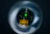
This work found that photons could be emitted on a chip by stretching a single-atom-thin layer of a semiconducting crystalline material (tungsten diselenide) around a gold nanocube — akin to stretching a sheet of cling film around a gaming die at a scale 500 times smaller than the width of a human hair. Positioned five nanometers above a gold mirror, the nanocube imprints quantum emitters onto the chip where the crystals strain against the cube’s corners, firing off photons one at a time. The cube and mirror funnel the photons into the tiny gap between them, concentrating their energy into a stream of photons that can be emitted quickly at a defined location.
Strauf’s discovery improved the average rate of photons created from one in 100 triggers to an astonishing one in two, making it the first practical, scalable method for generating quantum light sources on demand.
Doubling up
The more strain applied to the crystalline material, the more photons are emitted per second, and the brighter the light becomes. More strain also creates longer light wavelengths, shifting them closer to the range needed for free-space communication.
But the amount of strain necessary to reach these wavelengths is too much for a single layer of tungsten diselenide to withstand.
"When you reach wavelengths of about 750, the material breaks. The nanocube’s corners pierce through and punch a hole, and then there's no light," Strauf explained.
To solve the problem, Strauf, who is also director of the Nanophotonics Lab, turned to a practical solution: stacking a second layer of material on top of the first. By doing so, the researchers were able to increase strain on the crystal to shift emission wavelengths by more than 100 nanometers to 810 nanometers, ultimately achieving the desired infrared range.
Most Recent


NewsFlash
Industry Pioneers
Editor's Picks
-

European Consortium QUARTERNEXT Launches to Advance Next-Generation Quantum-Safe Communications for Industrial Deployment and Certification
-

IQM Selected to Deliver the LUMI-IQ Quantum Computer
-
NSF Launches Project Triad to Advance Quantum Technology for Real-World Applications
-
A New Ultra-Compact Sensor Paves the Way for More Powerful and Scalable Silicon Quantum Processors