New Platforms for Ultraconfined Plasmons and Optical Coupling to External Light
June 25, 2024 -- One of the biggest challenges in nanophotonics is the confinement of light inside small cavities. However, a small length scale is not the only desired property. Together with large lifetimes of the stored light and being able to work in the near-infrared frequency regime, they configure three essential features of the dreamed nanocavity that no one has simultaneously and efficiently accomplished yet.
There are many different types of materials and physics mechanisms available to build nanocavities. A promising approach is offered by the use of metals and the plasmon excitations (collective electron oscillations in the material) that they can support . Plasmons present two major advantages: they lie in the near-infrared regime, a spectral range of technological interest, and they offer an intrinsically high degree of confinement. Yet, confining photons for large lifetimes, a property generally quantified through the so-called quality factor, remains a challenge.
One of the main reasons preventing wider exploitation of confined plasmons is their poor coupling to light. The cause relies on the disparity between the wavelength of plasmons (short because of the ultra-confinement they are being forced to) and light (larger). A conventional way to circumvent this obstacle consists in what is called “laterally structuring the material’s surface”. Indeed, the coupling increases but at the cost of modifying the cavity itself.
In a recent work published in Advanced Materials by researchers at ICFO, together with collaborators of the Materials Physics Center (CSIC-UPV/EHU), Basque Country University and Al-Azhar University, a few-atomics-layer-thick (less than 3nm) crystalline silver nanostructure was built, achieving higher quality than other cavities of similar thickness (a factor of the order of 10 compared to the 2-3 achieved by traditional techniques). Their results were obtained thanks to the new fabrication process, where they first lithographically introduced the lateral shapes on a silicon wafer and then evaporated silver films of epitaxial quality, obtaining ultrathin crystalline metal layers. This way, the team was able to reduce the detrimental effect of the imperfections.
Despite their major advances, the researchers wanted to go one step further. It seemed that the patterning process was fundamentally hindering the production of cavities with an even higher degree of quality and confinement, both simultaneously. That is when they decided to approach the problem from a different perspective. Instead of trying to reduce the imperfections introduced by the lithography, they left the surface of the cavity flat (avoiding the defects) and focused on increasing the coupling between light and plasmons.
The initial idea of ICREA Prof. at ICFO Javier García de Abajo and his group members Saad Abdullah, Eduardo J. C. Dias, Jan Krpenský and Vahagn Mkhitaryan materialized in a successful experiment, now published in ACS Photonics. In this study, they demonstrate a new method that couples light to flat surface plasmons more effectively than previous strategies.
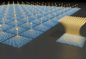
The experiment set-up consisted in the following: gold disks separated by a silica spacer from a planar gold surface. Plasmons lived in the latter and the goal was to couple incident light with them.
To achieve this, a dipolar scatterer was introduced, a rather indispensable element as it assisted the otherwise inefficient light-to-plasmon coupling. The gold disks were in charge of doing this job and, so, the distance between them and the gold flat surface played a crucial role. As Saad Abdullah, the first author of the paper, says: “Pretty soon we understood that we needed a scatterer to mediate and assist the coupling of light to plasmons, but we were limited in our knowledge of where to place it”.
In the end, they managed to demonstrate that there was a separation that maximized the coupling of incoming light to the plasmons underneath. However, the optimal distance varied depending on whether the disks were far apart from each other (so that interactions between them were forbidden) or placed closer (allowing those interactions). In the first case, the scatterers needed to be around 150 nanometers away from the gold surface, while in the second scenario, the best separation turned out to be five times shorter. This big difference highlights the influence of the interactions between scatterers when engineering light-to-surface coupling.
To sum up, the research group has provided two different strategies to face the same problem, both of them being an important step forward towards long-lived ultra-confinement of light. “The first approach aims at having high-quality crystalline silver thin films that have a lower loss and allow for a high confinement, whereas the second one aims to optimize parameters that allow for the maximum fraction of the light coupled to plasmons”, explains Abdullah.
Now, the increased quality of plasmonic films they have provided may enhance the efficiency of plasmonic solar cells and photothermal detections, helping to improve diagnostics by limiting the losses associated with this equipment. As Prof. García de Abajo finally remarks: “We have been able to successfully find new alternatives to understand light confinement in nanocavities from different perspectives. These results pose a major step forward in nanoplasmonic applications in optoelectronics, optical sensing, and the exploration of quantum-optics phenomena at the few-nanometer length scale”.

