Imec Successfully Integrates Colloidal Quantum Dot Photodiodes (QDPDs) on Metasurfaces Developed on 300mm CMOS Wafers
LEUVEN (Belgium), December 11, 2025 -- This week, at the IEEE International Electron Devices Meeting (IEDM 2025), imec, a world-leading research and innovation hub in advanced semiconductor technologies, successfully demonstrated the integration of colloidal quantum dot photodiodes (QDPDs) on metasurfaces developed on its 300 mm CMOS pilot line. This pioneering approach enables a scalable platform for the development of compact, miniaturized shortwave infrared (SWIR) spectral sensors, setting a new standard for cost-effective and high-resolution spectral imaging solutions.
Unlocking new possibilities in SWIR sensing
Short-wave infrared (SWIR) sensors offer unique capabilities. By detecting wavelengths beyond the visible spectrum, they can reveal contrasts and features invisible to the human eye and can therefore see through certain materials such as plastics or fabrics, or challenging conditions like haze and smoke. Conventional SWIR sensors remain, however, expensive, bulky, and challenging to manufacture, restricting their use to niche applications. Quantum dot (QD) image sensors, a new class of SWIR sensors, offer a promising alternative, combining lower cost with higher resolution. So far, however, they have operated in broadband rather than in spectral mode.
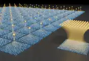
Imec addresses this challenge by successfully cointegrating colloidal quantum dot photodiodes (QDPDs) with metasurfaces developed on its 300 mm CMOS pilot line. Quantum dots are nanoscale semiconductors that can be tuned to absorb specific infrared wavelengths, while metasurfaces are nano-patterned ultra-thin layers that precisely control how light interacts with the sensor. By combining these elements in a CMOS-compatible process, imec has created a scalable platform for miniaturized SWIR spectral detectors, delivering a compact, high-resolution sensor architecture that can be manufactured using standard CMOS processes.
“What particularly sets this technology apart is its scalability,” says Vladimir Pejovic, R&D project lead at imec. “Traditional quantum dot image sensors require redesigning complex photodiode layers for every wavelength, which makes adjustments to each application’s spectrum complex and costly. Our approach shifts that complexity to the CMOS level, using metasurfaces to tune spectral response instead of altering the photodiode stack. This opens the door to easily customizable high-resolution spectral SWIR sensors and paves the way for new features in areas such as security, agriculture, automotive, aerospace, and beyond.”
Accelerating innovation through collaboration
This breakthrough is the result of a multidisciplinary effort, uniting imec’s expertise in quantum dot image sensors, flat optics (metasurfaces), and spectral imaging. The next step is to scale this technology from proof of concept to low volume, and ultimately, full-scale manufacturing. To accelerate this transition, imec invites partners to collaborate.
“Our ambition is to turn this breakthrough into an industry-ready platform,” Pawel Malinowski, imec portfolio manager, explains. “We want to work with partners to develop custom image sensors and integrated devices, demonstrating this technology in real-world applications. By combining imec’s spectral expertise, quantum dot know-how, and advanced CMOS process capabilities with specific application domains, we aim to accelerate innovation and bring next-generation SWIR sensors from proof-of-concept to full-scale manufacturing. Imec therefore welcomes collaboration with partners to help shape the future of sensing and imaging together.”
Topics:
Most Recent


NewsFlash
Industry Pioneers
Editor's Picks
-

Infleqtion to Deploy Fault-Tolerant Neutral-Atom Quantum Computer in Illinois
-

Start of IBERIANQCI, the Quantum Communications Infrastructure of the EuroQCI Program for Spain and Portugal
-

NIS 100 Million to Establish a National Quantum Computing R&D Infrastructure
-

OptQC and AIST Commence Initial Operations of "MoQuren," OptQC's First Optical Quantum Computer