Breakthrough Set to Push AI and Quantum Technologies Even Further
In research published in ACS Nano, TMOS researchers describe a solution to the on-chip light source problem that will significantly increase the integration density of photonic chips and lead to vastly higher processing powers. This will enable emerging technologies such as highly sophisticated AI and quantum computing to operate on smaller devices, such as mobile phones.
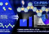
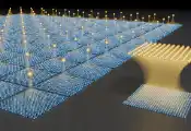
The researchers have grown microring lasers using a bottom-up approach. These microring lasers are only five micrometers in diameter with quantum wells inside each ring. These quantum wells enable the microring lasers to operate at wavelengths suitable for information telecommunications. They can adjust the wavelength of the lasers by controlling the thickness and composition of the quantum well. Each of the 2mm x 2mm samples they fabricated contained approximately 1000 microring lasers with fabrication yield exceeding 80%, demonstrating chip-scale manufacturing capability.
Previous attempts at microring lasers for communication purposes used top-down or transfer methods of fabrication, where the microring laser was etched out of a substance, similar to how statues are carved out of marble. These methods created rough surfaces on the quantum wells that made them highly inefficient, and limited the device performance, especially for laser dimensions. The TMOS researchers used a method called selective area-metal organic chemical vapour deposition (SA-MOCVD) to simultaneously ‘grow’ thousands of highly efficient lasers from the bottom layer up.
Lead author Wei Wen Wong says, “Recent decades have seen an exponential growth in data capacities of photonic chips, however on-chip light sources that enable high integration density of these photonic integrated circuits have remained elusive, primarily due to fabrication challenges. Our method successfully grows quantum wells with excellent crystal quality and morphology that conforms to the microring cavity. Importantly, it does not require any post-growth cavity etching.
“We solve numerous long-standing issues in the community, making this a breakthrough towards the realization of integrated micro-lasers and the huge step forward in miniaturizing devices for data-demanding technologies such as quantum computing.”
These microring lasers have a tunable wavelength emission in the telecommunication O-band, which is compatible with the wavelength used by other devices in the data transfer chain, such as 5g cell towers. Importantly, they have an efficacy of over 80% across the device. The impact of this technology will include faster internet speeds, faster computing, and an explosion in the Internet of Things, which requires enormous amounts of data transfer.
The results were underpinned by a rigorous analysis by researchers at The University of Manchester led by Dr. Stephen Church and Dr. Patrick Parkinson, who used an AI algorithm to measure the light output from the thousands of microrings and construct a dataset that shows the consistency of the growth process across the entire chip.
Wong says, “The contribution from the team at Manchester University allows us to demonstrate the high quality of the full sample set, rather than just a few individual examples, which gives an added layer of confidence in the scalability of our fabrication process.”
TMOS Chief Investigator Hark Hoe Tan says, “The next steps for this research will be to fabricate these lasers that can be electrically powered and also on silicon wafers as many photonic chips are made on this platform.
Most Recent


NewsFlash
Industry Pioneers
Editor's Picks
-

Infleqtion to Deploy Fault-Tolerant Neutral-Atom Quantum Computer in Illinois
-
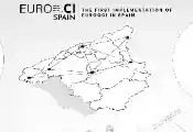
Start of IBERIANQCI, the Quantum Communications Infrastructure of the EuroQCI Program for Spain and Portugal
-

NIS 100 Million to Establish a National Quantum Computing R&D Infrastructure
-
OptQC and AIST Commence Initial Operations of "MoQuren," OptQC's First Optical Quantum Computer