Imec Developing 300mm Process for Quantum Qubits
Belgian r&d lab imec is developing a stable 300mm wafer process for making spin qubits and is developing a version using EUV lithography.
“We can make systems with hundreds of qubits but in order to have a real useful quantum computer we will have to scale up a lot more. Right now we have about 10 spin qubits but they have the potential to scale,” said Sofie Beyne, r&d project leader at imec.
“At imec we are focussing on making better spin qubits and the control of the qubits. To make a scalable system you need a uniform qubit to qubit and that is hard to achieve in a university lab. The question at imec is how to go from the design to a real device, so the imec fab can step in to use its existing CMOS 300mm wafers to achieve much better qubits,” she said.
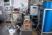
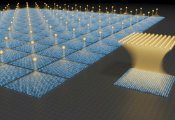
This process currently uses CMOS electron beam technology with overlapping gates to build a qubit of 100nm in a magnetic field. These are diced, bonded to a PCB and characterised at 10mK.
“We looked at different gate stack materials and different types of etching to optimise the electron mobility and the charge noise,” she said. This produces consistent devices with a fidelity of 99.9% which is very close to the best lab devices.
However imec is developing a mass production process with extreme UV lithography she said at the imec technology forum (ITF) today in Antwerp. “We are developing an EUV process to reduce misalignment between gates and process full 300mm wafers,” said Beyne.
imec is also looking at improving the fidelity and reducing the charge noise further by using a purer form of silicon wafer that has not been previously doped.


