‘Designer’ Superconducting Diamond Offers Roadmap to Multifunction Quantum Chips
July 2, 2026 -- UNIVERSITY PARK, Pa. — Diamond is extremely valuable to science and technology not for its sparkle but for its extreme hardness, ability to transfer heat, transparency to a large fraction of the light spectrum and a host of other exceptional properties. Two decades ago, scientists discovered another advantage: under the right conditions, diamond can become a superconductor — allowing electricity to flow through it with zero resistance.
Until recently, though, they knew little about how that happens, limiting its use in high-tech applications.
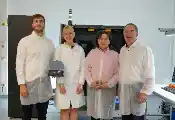
Now, in a study published in Proceedings of the National Academy of Sciences, researchers from Penn State, the University of Chicago Pritzker School of Molecular Engineering (UChicago PME) and the U.S. Department of Energy National Quantum Information Science Research Center Q-NEXT, led by Argonne National Laboratory, have uncovered new insights into the physics behind the phenomenon. The team carefully created high-quality diamond, allowing them to isolate its electronic signature from background material noise and revealing the fundamental mechanisms underlying its superconductivity that had long remained hidden.
“Understanding the underlying principles behind superconductivity in diamond could allow us to move beyond simply observing it to actively engineering it,” said Nitin Samarth, Verne M. Willaman Professor of Physics and of Materials Science and Engineering at Penn State and co-corresponding author of the paper.
The study offers a potential roadmap for enabling multiple functions on one quantum chip, an innovation that could make quantum technologies more efficient and better able to integrate with classical technologies, the researcher said. The key is in the capabilities of different kinds of qubits, or quantum bits, which are the building blocks of quantum technologies. Right now, it can be difficult to connect quantum technologies with disparate qubits but enabling them both in a single material — particularly a thermally efficient semiconductor as versatile as diamond — could have powerful implications.
“This offers a new way of thinking by integrating superconducting and semiconductor behavior to create opportunities for multifunction quantum devices,” said David Awschalom, the Liew Family Professor of Quantum Science and Engineering and Physics at UChicago PME, the director of the Chicago Quantum Exchange and co-corresponding author of the paper. “Imagine a future technology that combines light, spin, superconductivity and magnetism, all in a single material that one could also integrate with today’s microelectronics. There’s enormous potential at the interface between these nominally disparate areas of science that may be developed through a deeper physical understanding of the system through precise atomic-scale engineering.”
How it works
In order to become superconducting, diamond must be “doped” with atoms of boron. Doping is the process of adding different atoms to a host material to control or change certain properties, such as electrical conductivity.
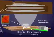
In the study, the scientists used a facility at Penn State’s Applied Research Lab to synthesize extremely high-quality diamond thin films doped with a random distribution of boron. Surprisingly, the research team found hidden order within this disordered distribution of boron in the form of a mosaic of superconducting “puddles.” These puddles, which might form from clustering of boron atoms within the diamond, eventually link up to allow electricity to flow without resistance, which they described as “granular superconductivity.” Even in microscopically uniform films, the superconductivity was found to be granular. More importantly, the researchers said, the superconducting mosaic is seemingly tunable and can be stretched and skewed by changing the magnetic field, electrical current and temperature.
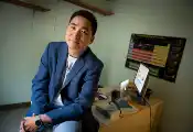
“Jyotirmay Dwivedi, the graduate student leading the project, discovered complex patterns in the electrical behavior of the films that could only be explained by intrinsic granularity,” Samarth said. “This serendipitous discovery caught us totally by surprise because these are structurally homogeneous, crystalline films! So, the question was: Where is this granularity coming from?”
By identifying how electrons move through and between these superconducting puddles, scientists can now begin to "stitch" these superconducting puddles together more effectively, which could significantly boost the performance and temperature range of future quantum devices. Currently, these systems require extreme cooling to function; raising that temperature would make quantum technology more accessible and energy efficient, the researchers said.
Potential for new innovations
One of the most exciting implications of this research, Awschalom said, is the potential for multifunctional “quantum-on-chip” applications, where multiple different types of quantum information technologies — like quantum communication and quantum computing — could co-exist and work together on a single diamond chip. This is due to diamond’s built-in “spin-photon interface,” meaning it naturally connects light to matter without any other technology necessary.
As the quantum industry looks to develop a domestic diamond supply chain, this “all-in-one” diamond platform offers a path toward chips that are not only more powerful but also easier to integrate with the classical high-frequency electronics used today.
These applications are only possibilities, but the study has taken a critical step, the team said.
“We now have a reliable roadmap for engineering diamond superconductors by independently adjusting the material’s core properties,” Samarth said. “By tuning parameters like boron doping density, crystalline orientation, mechanical strain and dimensionality, we can move beyond simple observation and start designing diamond superconductors for specific roles. There are a lot of exciting possibilities here, for both quantum and classical technology.”
Topics:
Most Recent