A Novel Universal Light-Based Technique to Control Valley Polarization in Bulk Materials
Electrons inside solid materials can only take certain values of energy. The allowed energy ranges are called “bands” and the space between them, the forbidden energies, are known as “band-gaps”. Both of them together constitute the “band structure” of the material, which is a unique characteristic of each specific material.

When physicists plot the band structure, they usually see that the resulting curves resemble mountains and valleys. In fact, the technical term for a local energy maximum or minimum in the bands is called a “valley”, and the field which studies and exploits how electrons in the material switch from one valley to the other is coined “valleytronics”.
In standard semiconductor electronics, the electric charge of the electrons is the most used property exploited to encode and manipulate information. But these particles have other properties that could also be used for the same purpose, such as the valley they are in. In the past decade, the main aim of valleytronics has been to reach the control of valley population (also known as valley polarization) in materials. Such an achievement could be used to create classical and quantum gates and bits, something that could really drive the development of computing and quantum information processing.
Previous attempts presented several drawbacks. For example, the light used to manipulate and change valley polarization had to be resonant, that is, the energy of its photons (the particles that constitute light) had to correspond exactly to the energy of the band-gap of that particular material. Any small deviation reduced the efficiency of the method so, provided that each material has their own band-gaps, generalizing the proposed mechanism seemed something out of reach. Moreover, this process had only been achieved for monolayer structures (2D materials, just one-atom-thick). This requirement hindered its practical implementation, as monolayers are usually limited in size, quality and difficult to engineer.
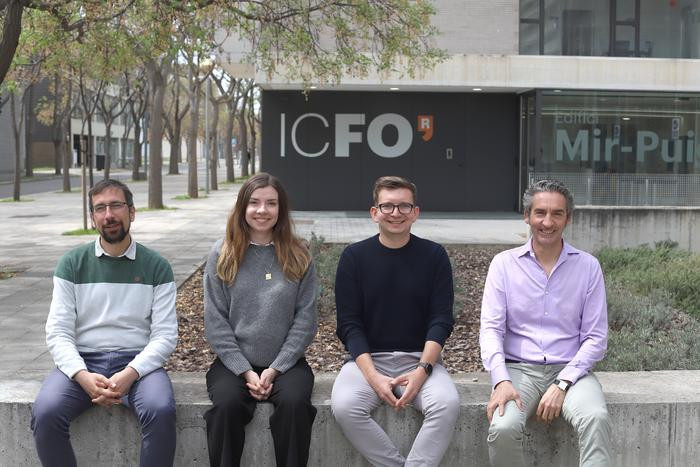
Now, ICFO researchers Igor Tyulnev, Julita Poborska, Dr. Lenard Vamos, led by Prof. ICREA Jens Biegert, in collaboration with researchers from the Max-Born-Institute, the Max-Planck Institute for the Science of Light, and Instituto de Ciencia de Materiales de Madrid have found a new universal method to induce valley polarization in centrosymmetric bulk materials. The discovery, published in Nature, unlocks the possibility to control and manipulate valley population without being restricted by the specific chosen material. At the same time, the method can be used to obtain a more detailed characterization of crystals and 2D materials.
Valley polarization in bulk materials is possible
The adventure began with the experimental group led by ICREA Prof. at ICFO Jens Biegert who initially wanted to experimentally produce valley polarization using their particular method in 2D materials, following the lines of what had been theoretically proved in a previous theoretical paper by Álvaro Jiménez, Rui Silva and Misha Ivanov. To set up the experiment, the initial measurement was tried on bulk MoS2 (a bulk material is made of many monolayers stacked together) with the surprising result that they saw the signature of valley polarization. “When we started working on this project, we were told by our theory collaborators that showing valley polarization in bulk materials was rather impossible”, explains Julita Poborska.
The theoretical team remarks as well how, at the very beginning, their model was only suitable for single 2D layers. “At a first glance, it seemed that adding more layers would hinder the selection of specific valleys in the sample. But after the first experimental results, we adjusted the simulation to bulk materials and it validated the observations surprisingly well. We did not even try to fit anything. It is just the way it came out”, adds Prof. Misha Ivanov, the theorist leader. In the end, “it turned out that yes, you can actually valley polarize bulk materials that are central symmetric, because of the symmetry conditions”, concludes Poborska.
As Igor Tyulnev, first author of the article, explains, “our experiment consisted in creating an intense light pulse with a polarization that fitted this internal structure. The result was the so-called “trefoil field”, whose symmetry matched the triangular sub-lattices that constitute hetero-atomic hexagonal materials”.
This symmetry-matched strong field breaks the space and time symmetry within the material, and, more importantly, the resulting configuration depends on the orientation of the trefoil field with respect to the material. Therefore, “by simply rotating the incident light field, we were able to modulate the valley polarization”, concludes Tyulnev, a major achievement in the field and a confirmation of a novel universal technique that can control and manipulate the electron valleys in bulk materials.
The experimental process
The experiment can be explained in three main steps: First, the synthesis of the trefoil field; then its characterization; and finally, the actual production of valley polarization.
The researchers emphasize the incredibly high precision that the characterization process required, as the trefoil field is made of not just one, but two coherently combined optical fields. One of them had to be circularly polarized in one direction, and the other needed to be the second harmonic of the first beam, polarized with the opposite handedness. They superimposed these fields onto each other, so that the total polarization in time traced the desired trefoil shape.
Three years after the initial experimental attempts, Igor Tyulnev is thrilled by the recent Nature publication. The appearance in such a prestigious journal recognizes the new universal method which, as he states, “can be used not only to control the properties of a wide variety of chemical species, but also to characterize crystals and 2D materials”.
As Prof. ICREA at ICFO Jens Biegert remarks: “Our method may provide an important ingredient to engineer energy efficient materials for efficient information storage and fast switching. This addresses the pressing need for low-energy consumption devices and increased computational speed. I cannot promise that what we have provided is THE solution, but it is probably one solution on this big challenge”.


