
Argonne’s Advanced Photon Source Illuminates the Quantum World Within Materials
November 16, 2026 — Within every material is a hidden world — a sea of atoms and electrons in motion. At this scale, matter doesn’t play by the classical rules we are used to. Instead, it’s governed by the much stranger rules of quantum mechanics.
In the quantum realm, objects can seem to exist in two places at once, affect each other across great distances and tunnel through otherwise impenetrable barriers. In general, we observe quantum phenomena only at the scale of atoms and fundamental particles. But in some materials, quantum behavior emerges at scales much larger, leading to unexpected and useful material states and properties.
“You don’t have to be an X-ray expert to take advantage of the APS. Users can bring their science, and we provide the capabilities and expertise to help them get the answers they’re looking for.” — Matthew Highland, APS physicist and group leader
These are called quantum materials, and they could form the basis for lighter, better, smaller and more energy-efficient materials and technologies. In particular, quantum materials show great promise for use in future quantum information technologies, such as powerful quantum computers that are expected to solve intractable problems and sensors that may be able to detect disease in a single cell of human tissue.
But turning this potential into reality requires a deeper understanding of how these materials work and how to create and control them. At the Advanced Photon Source (APS) — a U.S. Department of Energy (DOE) Office of Science user facility at DOE’s Argonne National Laboratory — researchers are using some of the world’s most powerful X-ray capabilities to watch quantum materials in action and uncover the mechanisms behind their remarkable properties.
The APS acts as a scientific Swiss Army knife for materials research, providing a suite of tools for scientists to look at samples from different perspectives. These tools can detect even the most elusive clues hidden within a material’s smallest structures, such as sudden shifts in a crystal’s symmetry, the fleeting signature of an electron’s activity or a subtle response to a changing environment.
“Whether they’re from universities, national laboratories or industry, we want researchers to come here with challenging questions and leave with new understanding,” said Matthew Highland, a physicist and group leader at the APS. “You don’t have to be an X-ray expert to take advantage of the APS. Users can bring their science, and we provide the capabilities and expertise to help them get the answers they’re looking for.”
Seeing more with an upgraded APS
At the APS, electrons travel around a large ring at near the speed of light. As the electrons are steered around bends in the ring, they emit X-ray beams that travel down beamlines to dozens of experimental stations, where researchers probe everything from proteins to batteries.
After a recent major upgrade, the APS produces X-ray beams up to 500 times brighter than before, making it the brightest synchrotron X-ray light source in the world. The upgrade also increased the coherence of the X-rays. Like the light from a laser, coherent X-rays remain in phase — or synced up — with one another as they travel to the sample.
“With less coherent beams, we could measure the average properties of a material, but the increased coherence allows us to detect small variations hidden within that overall picture,” Highland said. “We can see subtle differences between tiny regions within a sample and watch them evolve over time.”
The increased coherence also allows researchers to focus the X-ray beam onto much smaller spots. Many quantum materials are difficult to fabricate, and the most interesting regions may be only a few micrometers across — the width of a strand of a spider’s web. Rather than requiring large, nearly perfect crystal samples, scientists can now examine tiny crystallites embedded within more complex samples, accelerating the search for promising new materials.
The upgrade also enables scientists to study quantum materials under more realistic conditions. The higher-energy X-rays can penetrate deeper into sample environments, allowing researchers to peer through the walls of experiment chambers and other equipment while materials are being synthesized, heated, cooled, compressed or exposed to magnetic fields. As opposed to capturing only static snapshots, scientists can watch these materials evolve in real time, revealing how their quantum behavior emerges and changes.
Watching quantum materials take shape
One of the newest beamlines at the APS was built specifically to capitalize on the facility’s upgraded capabilities. The Coherent High-Energy X-ray (CHEX) beamline at 28-ID combines highly coherent, high-energy X-rays with specialized experimental setups.
In particular, the beamline is designed to actively observe samples during the growth process. These look-while-you-cook experiments are particularly valuable for studying quantum materials, whose final properties often depend on exactly how they are made. Tiny differences that develop during growth can dramatically affect how a material behaves.
For example, CHEX is helping researchers study the growth of silicon carbide, a material being explored as a host for quantum bits, or qubits, the basic unit of quantum information. Certain atomic arrangements within the material, known as polytypes, may provide especially promising environments for qubits. However, controlling which polytypes form during synthesis has proven difficult, since significantly different structures can form under very similar growth conditions.
As part of Q-NEXT — a DOE National Quantum Information Science Research Center led by Argonne — Highland and his collaborators are using the CHEX beamline to observe the growth of silicon carbide during a process called chemical vapor deposition, where the material is synthesized one layer at a time. The experiments are revealing how the sample’s atoms arrange themselves during the process, exposing complex dynamics that would otherwise remain hidden.
“Any time we’ve used in-situ X-ray beams to investigate a growth process, we’ve found that it is more complicated than the conventional wisdom suggests,” Highland said. “By watching the material as it grows, we can understand those local processes in a way that simply isn’t possible just by looking at the finished crystal.”
By identifying the conditions that produce specific polytypes, the researchers hope to develop recipes that can eventually be transferred to larger-scale manufacturing efforts. Experiments like these bring the nation closer to viable qubit platforms for use in quantum computers, sensors and other quantum information technologies.
Tracking transformations in quantum materials
Quantum materials are anything but static. Atomic irregularities migrate, magnetic features fluctuate, and exotic electronic states emerge, compete with each other and disappear. These subtle transitions often determine how a material behaves and whether it might be useful for future microelectronics or quantum information technologies.
Capturing those changes is the specialty of the X-ray Photon Correlation Spectroscopy (XPCS) beamline at 8-ID at the APS. Rather than taking a single snapshot of a material, XPCS follows its evolution, allowing researchers to watch fluctuations unfold across timescales ranging from millionths of a second to many minutes.
“Unlike a lot of the better-understood materials that power much of our present technology, quantum materials aren’t uniform. They vary significantly over time, and from one tiny region to the next,” said Yue Cao, a physicist in Argonne’s Materials Science division and an XPCS beamline user. “XPCS is helping us determine how these fluctuations influence overall material properties, such as electric conductivity, magnetism and decoherence in quantum information systems.”
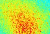
The XPCS beamline takes advantage of the highly coherent X-ray beams produced by the upgraded APS. When coherent X-rays scatter from a material, they leave behind features in the experimental data — called speckles — that change as the material changes.
“By tracking how the speckles evolve, researchers can uncover activity within a sample down to the atomic scale,” said Suresh Narayanan, a physicist and group leader at the APS.
One area where XPCS is making an impact is the study of a class of quantum materials called complex oxides. These materials can switch between different states — for example, from conducting to insulating, or from magnetic to nonmagnetic — when exposed to changes in temperature, mechanical strain or electric and magnetic fields.
Researchers are finding that tiny defects, such as missing oxygen atoms within these materials’ atomic structures, often play a significant role in driving their transformations. Using XPCS, scientists can watch these defects move and organize themselves in real time while the materials shift from one state to another. Revealing the mechanisms behind phase transitions is key to designing materials with properties that can be precisely controlled.
XPCS is also helping researchers explore materials for neuromorphic devices, which mimic aspects of how the brain processes and stores information. In these systems, a material can continue to show the effects of a stimulus even after that stimulus is removed. This creates a kind of memory that is useful for computing applications such as complex pattern recognition and data analysis.
“These dynamics are often very subtle and can occur over a wide range of time scales,” said Zahir Islam, a physicist at the APS. “XPCS is specially equipped to track how memory in these materials forms and fades over time, which is essential for designing neuromorphic devices for different kinds of computing tasks.”
Pushing quantum materials to their limits
Many quantum materials reveal their most interesting properties only under extraordinary conditions. Cooling them to temperatures near absolute zero, exposing them to intense magnetic fields or squeezing them under enormous pressure can fundamentally change how their electrons behave, causing entirely new quantum states to emerge.
Exploring these transformations requires more than simply shining X-ray beams on a sample. Researchers need to measure subtle changes in a material’s electronic and magnetic properties while those extreme conditions are being applied. At the APS’s Polarization Modulation Spectroscopy (POLAR) beamline at 4-ID, scientists do this by combining specialized sample environments with precisely controlled X-ray beams.
In particular, the POLAR beamline can manipulate the X-ray beam’s polarization, or the pattern with which the light waves oscillate as they travel. This affects how the beam interacts with a material. By changing the polarization — for example, rotating it clockwise or counterclockwise — researchers at POLAR can make different aspects of a material stand out, allowing them to probe electronic and magnetic properties with exceptional sensitivity.
This polarization control pairs well with the unique sample environments at the beamline, which push materials to their physical limits during X-ray experiments. Tiny crystals can be compressed between the flattened tips of two diamonds, which generate pressures exceeding 1 million atmospheres — similar to the pressures within Earth’s core. At POLAR, scientists can also examine materials at cryogenic temperatures or under powerful magnetic fields.
After the upgrade, the beamline can produce polarized X-ray beams that are far brighter and more coherent than before and can focus them onto spots more than 100 times smaller than the width of a human hair.
In recent experiments led by DOE’s Oak Ridge National Laboratory, researchers used the tightly focused, polarized X-ray beams at POLAR to image a quantum material with promising magnetic properties. When cooled to cryogenic temperatures, this material can reorganize itself in surprising ways, shifting between various magnetic states. Some of those states are chiral.
“You can think of an electron as a tiny magnet, and an electron’s spin represents the orientation of that magnet,” said APS physicist Gilberto Fabbris. “In a chiral state, the spins of the electrons in the material rotate in a certain direction, forming a sort of spiral pattern across the sample.”
By scanning the sample point by point with both clockwise- and counterclockwise-polarized X-ray beams, the team mapped where those chiral structures appeared and how they changed. They found that the direction of the chiral patterns could spontaneously flip as the temperature changed, unless strain in the material held them in place.
“Chiral states hold promise for a variety of applications, such as energy-efficient computing and memory,” Fabbris said. “By making magnetic and electronic states visible, POLAR is helping us understand how these complex quantum phases emerge and interact under different conditions.”
Harnessing quantum phenomena for better detectors
The quantum world is not only a subject of research at the APS. Quantum phenomena are also helping scientists build the next generation of tools for exploring materials.
Antonino Miceli, a physicist and group leader at the APS, leads a team developing quantum-enhanced detectors that capture X-rays with extraordinary sensitivity. These detectors use quantum phenomena to amplify the faint signals produced during X-ray experiments.
When an X-ray beam strikes a detector, it deposits a tiny amount of energy, causing a small temperature change. Measuring that change allows scientists to determine the energy of the incoming photon, revealing information about the material that scattered it. But these signals are incredibly small, and traditional amplifiers can obscure them with background noise.
By harnessing quantum effects within superconducting materials, Miceli’s team is building ultrasensitive detectors capable of sensing and amplifying these subtle changes while minimizing noise.
In the future, Miceli envisions these quantum sensors becoming more than just X-ray detectors. By placing them directly next to the samples during experiments, researchers can combine X-ray measurements with other signals from the materials, such as heat capacity — or how readily a material changes temperature in response to added energy.
“A lot of phase transitions cause jumps in heat capacity, so if we can monitor that alongside X-ray scattering data, we can identify things that we can’t see with X-rays alone,” Miceli said.
Together, the instruments at the APS form a powerful toolkit for exploring quantum materials. Whether watching crystals grow, tracking fluctuating quantum states or developing quantum-enhanced detectors, APS staff and users are bringing the quantum world into sharper focus and contributing to the development of technologies once thought impossible.
This research is supported in part by DOE’s Office of Basic Energy Sciences, including its Materials Science and Engineering division and Scientific User Facilities division. Additional contributors to this article include Eric Dufresne, Dillon Fong, Lisa Gades, Tejas Guruswamy, Elliot Kisiel, Jessica McChesney, Umeshkumar Patel, Orlando Quaranta and Jörg Strempfer.
Most Recent









Editor's Picks
-

NEC and IBM Japan Successfully Demonstrate Japan's First PQC and QKD Integrated Method for Quantum-Safe Communication Technology
-

NVIDIA Announces Collaboration With IBM and Fermi National Accelerator Laboratory To Launch Quantum-Classical Codesign Platform, Plus Error-Correction Breakthrough To Advance Practical Quantum Computing
-

Infleqtion Reports Third Quarter 2026 Record Revenue Results, Achieves 30-Logical-Qubit Milestone and Maintains Full-Year Revenue Guidance
-

IBM, AMD Advance Quantum Error Correction Decoding at Scale