Lead-Vacancy Centers in Diamond as Building Blocks for Large-Scale Quantum Networks
Much like how electric circuits use components to control electronic signals, quantum networks rely on special components and nodes to transfer quantum information between different points, forming the foundation for building quantum systems. In the case of quantum networks, color centers in diamond, which are defects intentionally added to a diamond crystal, are crucial for generating and maintaining stable quantum states over long distances.
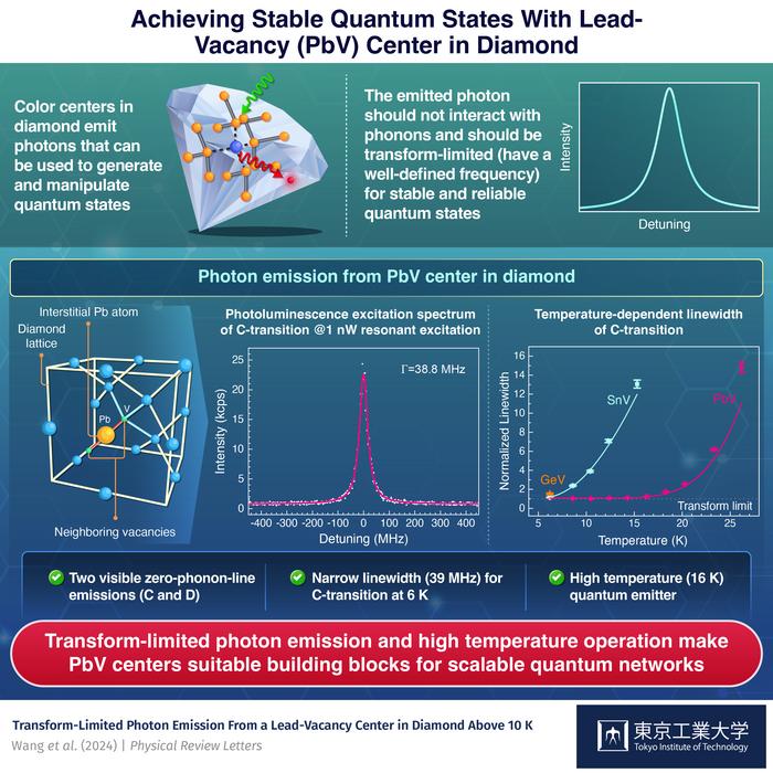
When stimulated by external light, these color centers in diamond emit photons carrying information about their internal electronic states, especially the spin states. The interaction between the emitted photons and the spin states of the color centers enables quantum information to be transferred between different nodes in quantum networks.
A well-known example of color centers in diamond is the nitrogen-vacancy (NV) center, where a nitrogen atom is added adjacent to missing carbon atoms in the diamond lattice. However, the photons emitted from NV color centers do not have well-defined frequencies and are affected by interactions with the surrounding environment, making it challenging to maintain a stable quantum system.
To address this, an international group of researchers, including Associate Professor Takayuki Iwasaki from Tokyo Institute of Technology, has developed a single negatively charged lead-vacancy (PbV) center in diamond, where a lead atom is inserted between neighboring vacancies in a diamond crystal. In the study published in the journal Physical Review Letters on February 15, 2024, the researchers reveal that the PbV center emits photons of specific frequencies that are not influenced by the crystal’s vibrational energy. These characteristics make the photons dependable carriers of quantum information for large-scale quantum networks.
For stable and coherent quantum states, the emitted photon must be transform-limited, which means that it should have the minimum possible spread in its frequency. Additionally, it should have emission into zero-phonon-line (ZPL), meaning that the energy associated with the emission of photons is only used to change the electronic configuration of the quantum system, and not exchanged with the vibrational lattice modes (phonons) in the crystal lattice.
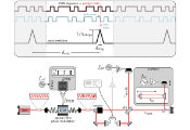
To fabricate the PbV center, the researchers introduced lead ions beneath the diamond surface through ion implantation. An annealing process was then carried out to repair any damage caused by the lead ion implantation. The resulting PbV center exhibits a spin 1/2 system, with four distinct energy states with the ground and the excited state split into two energy levels. On photoexciting the PbV center, electron transitions between the energy levels produced four distinct ZPLs, classified by the researchers as A, B, C, and D based on the decreasing energy of the associated transitions. Among these, the C transition was found to have a transform-limited linewidth of 36 MHz.
“We investigated the optical properties of single PbV centers under resonant excitation and demonstrated that the C-transition, one of the ZPLs, reaches the nearly transform-limit at 6.2 K without prominent phonon-induced relaxation and spectral diffusion,” says Dr. Iwasaki.
The PbV center stands out by being able to maintain its linewidth at approximately 1.2 times the transform-limit at temperatures as high as 16 K. This is important to achieve around 80% visibility in two-photon interference. In contrast, color centers like SiV, GeV, and SnV need to be cooled to much lower temperatures (4 K to 6 K) for similar conditions. By generating well-defined photons at relatively high temperatures compared to other color centers, the PbV center can function as an efficient quantum light-matter interface, which enables quantum information to be carried long distances by photons via optical fibers.
“These results can pave the way for the PbV center to become a building block to construct large-scale quantum networks,” concludes Dr. Iwasaki.

