Argonne, Sandia Scientists Create Qubits Using Precision Tools of Nanotechnology
January 18, 2024 -- Silicon carbide is becoming a major player on the quantum scene. Widely used in specialized electronics goods such as LEDs and electric vehicles, silicon carbide boasts versatility, wide commercial availability and growing use in high-power electronics, making it an attractive material for quantum information science, whose impact is expected to be profound.
Drawing on physics at the atomic scale, technologies such as quantum computers, networks and sensors will likely revolutionize areas as varied as communication, drug development and logistics in the coming decades.
Now, scientists at the U.S. Department of Energy’s (DOE) Argonne National Laboratory, DOE’s Sandia National Laboratories and partner institutions have carried out a comprehensive study on the creation of qubits — the fundamental units of quantum information processing — in silicon carbide.
In a first-of-its-kind study, the Argonne and Sandia scientists harnessed cutting-edge nanoscale research tools at the two labs and successfully demonstrated a method for implanting qubits in silicon carbide with extreme precision. They also carried out state-of-the-art analysis on how silicon carbide responds at the atomic scale to the qubits’ implantation.
Their high-precision investigations enable scientists to better engineer quantum devices for specific purposes, whether to design ultraprecise sensors or build an unhackable communication network.
The researchers’ work was published in the journal Nanotechnology and supported in part by Q-NEXT, a DOE National Quantum Information Science Research Center led by Argonne.
“We can better understand the molecular dynamics of the material, beyond the typical hand-waving explanation that we’re used to,” said Argonne scientist Nazar Delegan, who is the lead author on the paper. “We also showed that we can create spatially localized qubits in this very relevant material system, silicon carbide.”
Researchers are working to perfect the creation of qubits in silicon carbide. These qubits take the form of two side-by-side atom-sized holes, or vacancies, within the silicon carbide crystal. Scientists call this pair of atomic holes a divacancy.
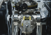
The group’s paper describes how they leverage a process perfected at Sandia’s Center for Integrated Nanotechnologies (CINT) to create the qubits. Using one of CINT’s nanoscale-materials tools, scientists were able to precisely implant silicon ions in the silicon carbide. The process knocks loose atoms in the silicon carbide, creating divacancies in the material.
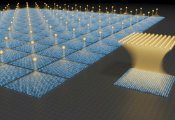
The process enables scientists not only to specify the exact number of atoms to inject into the silicon carbide, but also to position the divacancies at a precision of roughly 25 nanometers. Such precision is crucial for integrating quantum technologies into electronic devices.
“You don’t have to go on a hunt to find an atomic-scale vacancy in a larger piece of material,” said Michael Titze, Sandia scientist and the Sandia lead on the paper. “By using the focused ion beam, you can put the atom somewhere, and someone else can find the vacancy within a 100-nanometer scan. We’re making this stuff easier to find and, by extension, easier to study and incorporate into a practical technological platform.”
Following the precision positioning of the qubits, scientists at Argonne annealed — or heated — the silicon carbide samples to enhance the qubits’ properties and stabilize the silicon carbide crystal.
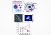
The team then precisely mapped, for the first time, the ways the divacancies formed within the crystal and changes in its nanoscale structure following the annealing process. Their tool for this characterization was Argonne’s powerful Advanced Photon Source (APS), a DOE Office of Science user facility.
The APS is a giant, ring-shaped machine large enough to encircle a sports stadium. It produces very bright beams of X-rays to peer deep inside materials.
Researchers at Argonne’s Center for Nanoscale Materials (CNM), also a DOE Office of Science user facility, used CNM’s dedicated X-ray beamline at the APS to study the mobilization and creation of divacancy qubits inside silicon carbide. How many vacancies are formed when you adjust the number of implanted atoms? What happens when you adjust the atom’s energy? How does the implantation affect the structure of the silicon carbide?
“These impurities lead to different crystal configurations, which lead to strain,” Titze said. “How does the strain get affected by these various defects?”
To answer such questions, the team focused a 25-nanometer-thin X-ray beam onto silicon carbide samples.
“You can scan across your implanted material, and at every single point, you’re able to get the structural information of what’s happening,” Delegan said. “So now you have an X-ray way of looking at these scales. You’re able to say, ‘How was the crystal behaving before, during and after implantation?’”
Using the CNM’s X-ray beamline at the APS, the group was able to image changes in the silicon carbide’s nanoscale structure with impressively high-resolution, detecting changes at 1 part per million.
By combining the precise positioning of qubits using Sandia’s CINT tool and the precise imaging of their crystal environment with Argonne’s APS and CNM, the team takes a significant step toward the creation of bespoke silicon carbide qubits, which is expected to lead to greater customizability for quantum applications. Their work also adds to the book on silicon carbide qubits, empowering the scientific community to develop and tune their silicon-carbide-based quantum devices in an intentional way.
“This work enables all these quantum information science applications where you want to implant a very specific ion because of its useful quantum properties,” Titze said. “You can now use this knowledge of local strain around the defects to engineer it in such a way that you can make, say, hundreds of defects on a single chip talk to each other.”
The team’s work is a testament to inter-institutional collaboration.
“We at CINT provide the capability for precise implantation of atoms,” Titze said. “And our colleagues at CNM and Q-NEXT provide a unique way to make them actually findable when they need to look for them.”
The researchers will continue to use the two labs’ nanoscale-materials tools to characterize the dynamics of creating qubits in silicon carbide.
“We were able to demonstrate the tools’ sensitivities,” Delegan said. “And the cool part is, with some extra experimental considerations, we should be able to start to extract interesting behaviors with those values.”
This work was supported by the DOE Office of Science National Quantum Information Science Research Centers as part of the Q-NEXT center.
This work was performed, in part, at the Center for Integrated Nanotechnologies, an Office of Science user facility operated for the DOE Office of Science. Work performed at the CNM and APS, both DOE Office of Science user facilities, was supported by the DOE Office of Basic Energy Sciences.


